AI Is Changing How Semiconductor Fabs Work — and Engineers Are Moving Faster Because of It
AI is transforming semiconductor manufacturing by accelerating simulations, enabling faster process optimization and reducing costly physical trials through digital twins and physics-based predictions.
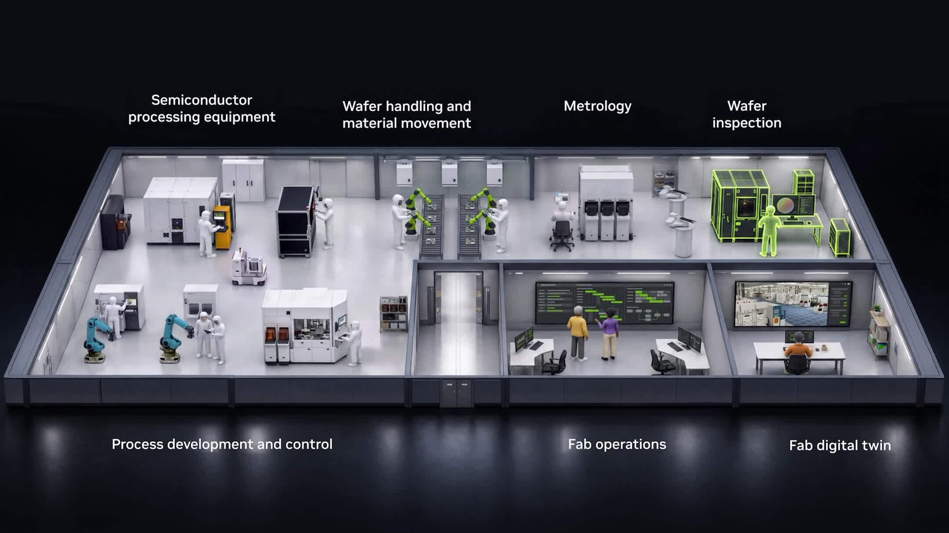
Demand for advanced chips is rising while manufacturing processes grow more complex, leaving engineers with critical but time-consuming tasks such as analyzing process changes and root causes. Physical experiments on fab lines are slow and expensive, and errors in yield or quality decisions carry real consequences. AI is reshaping semiconductor manufacturing by shortening simulation times, allowing engineers to evaluate more alternatives before committing to physical trials. Physics-based AI models predict process behavior without requiring full simulations each time, while AI agents automate sequences of engineering tasks that previously took hours.
Accelerated computing enables engineers to test more alternatives by speeding up calculations, with multiphysics simulations modeling interactions like heat transfer and electrical behavior. COMSOL, using NVIDIA’s cuDSS library, has accelerated semiconductor manufacturing simulations by up to 10 times, helping engineers optimize equipment and compare alternatives before physical testing. Applied Materials and NVIDIA’s collaboration integrates NVIDIA cuDSS into the Ginestra simulation platform, achieving up to 10 times faster runs than CPU-only approaches, and NVIDIA PhysicsNeMo delivers topography simulations up to 35 times faster.
Computational lithography, which defines circuit patterns on silicon, involves calculations too intensive for CPU-based production, but Siemens’ integration of NVIDIA cuLitho into its Calibre software delivers up to 17 times acceleration on key workloads. This expansion allows engineers to verify more scenarios before wafer production and explore material behaviors influencing next-generation processes. AI trained on physics can predict material and process behavior without full simulations, particularly valuable for complex calculations that remain costly even on accelerated hardware.
AI agents automate tasks such as selecting models for specific engineering challenges, reducing response times from hours to minutes, as demonstrated by Advantest using NVIDIA NeMo Switchyard. Digital twins built with NVIDIA Omniverse enable teams to simulate equipment configurations and process changes virtually, reducing experimentation costs and risks. Applied Materials uses these digital twins to model material movement, identify bottlenecks, and evaluate layouts and operating strategies across entire fabs.