JinkoSolar unveils 28%-efficient back-contact TOPCon solar cell with amorphous silicon heterojunction passivation
JinkoSolar introduced a back-contact TOPCon solar cell with amorphous silicon heterojunction passivation, achieving a peak efficiency of 28% and reducing optical shading losses by eliminating front-side metallization.
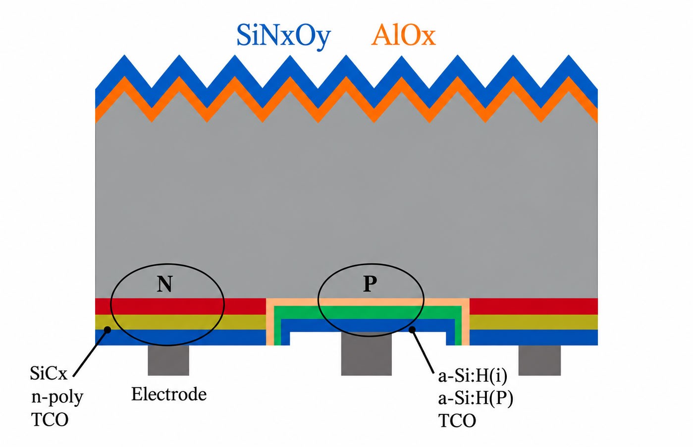
Chinese module manufacturer JinkoSolar announced its TOPCon-based Amorphous-Si Passivating Cell (TAC) technology at an event in Shanghai on Oct. 17, combining TOPCon electron-selective contacts with heterojunction hole-selective contacts on a rear-electrode layout. The design uses an n-type silicon wafer with alternating carrier-selective contact regions on the rear surface, removing front-side metallization to minimize optical shading losses. The architecture integrates a silicon oxide tunneling layer and doped polycrystalline silicon for electron transport, alongside intrinsic and doped hydrogenated amorphous silicon for hole collection, improving surface passivation and open-circuit voltage.
JinkoSolar’s TAC technology employs a transparent conductive oxide layer to enhance lateral carrier transport, with amorphous silicon passivation processes conducted below 200°C. High-precision laser patterning and dielectric isolation separate the electron and hole contact regions, while a ‘2+1’ design merges TOPCon electron contacts, HJT hole contacts, and rear-electrode structures. The company also developed the Global Passivation Process (GPP) to reduce recombination losses and MCP 2.0 to target carrier recombination at cut-cell edges through a cut-before-passivation sequence.
The white paper specifies a bulk minority-carrier lifetime exceeding 2 ms and a bulk recombination current density below 5 fA/cm² for the silicon substrate. JinkoSolar reported production cell efficiencies exceeding 27%, with a peak efficiency of 28%, though the white paper does not provide third-party certification or average production-line efficiency details. The announcement highlights TAC’s potential as a bottom-cell platform for perovskite-silicon tandem devices.
JinkoSolar identified low-temperature metallization and copper-containing contact materials as areas for further development, alongside the integration of TAC technology. The company’s Oct. 17 announcement did not link its previously reported third-party-certified 27.2% efficiency for an n-type back-contact research cell to TAC measurements, maintaining separate reporting for the two results.