Intel and Lens Technology Collaborate to Enable Advanced Semiconductor Packaging for the AI Era
Intel and Lens Technology will jointly develop glass substrate-based semiconductor packaging to enhance performance, power efficiency, and interconnect density for AI and data center applications.
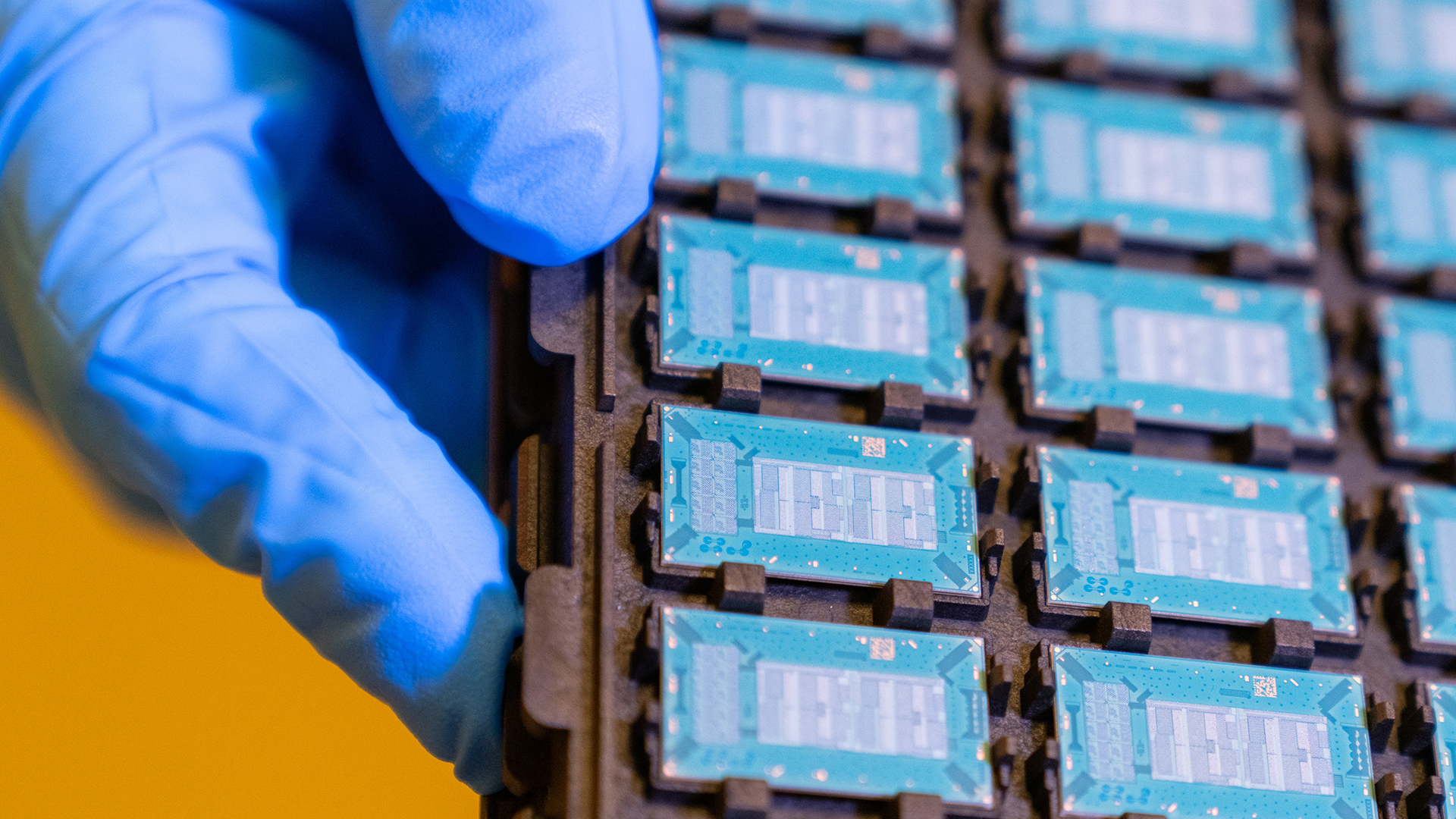
Intel Corporation and Lens Technology announced a strategic collaboration to advance semiconductor packaging using glass substrates. The partnership aims to improve performance, interconnect density, and power efficiency for future computing platforms, particularly in AI, data centers, and specialized computing. Intel highlighted the growing importance of advanced packaging in meeting AI system demands, while Lens Technology emphasized its expertise in precision glass processing and large-scale manufacturing. The companies will explore new approaches to packaging to support next-generation system-level innovation.
Lens Technology, known for advanced materials engineering and precision manufacturing, will contribute its capabilities in glass materials and high-precision laser processing to the collaboration. Intel will leverage its expertise in semiconductor design and packaging technologies. Together, they aim to accelerate innovation in advanced packaging to meet global demand for next-generation computing solutions and AI infrastructure. The partnership will focus on scaling critical manufacturing processes for advanced semiconductor packaging adoption.
The collaboration will explore potential areas of cooperation, including components for AI PCs, high-reliability solutions for data center servers, and hardware platforms for AI robotics, intelligent industrial equipment, and edge computing. Intel and Lens Technology will also assess additional areas where their complementary capabilities may align. The goal is to develop technologies that address the evolving needs of AI-driven applications across multiple sectors.
Intel Foundry’s existing technologies, such as Foveros stacking, EMIB silicon bridges, and EMIB-T, will inform the partnership’s efforts to scale chiplets and bypass reticle limits for high-volume manufacturing. The collaboration is expected to create permanent high-tech jobs and expand manufacturing capacity, including in Ireland. Investment in advanced packaging is projected to support domestic leadership in high-volume production while engaging specialized tradespeople.